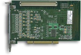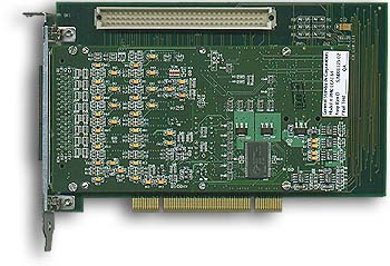
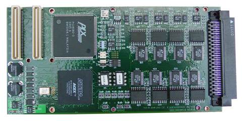
The 16-Bit PCI66-16AI64SSC analog input board samples and digitizes 64 input channels simultaneously at rates up to 200,000 samples per second for each channel. Each input channel contains a dedicated 16-Bit sampling ADC, and the resulting 16-bit sampled data is available to the PCI bus through a 1 MByte FIFO buffer. The 32-Bit local data path supports full D32 local-bus data packing. Throughput capacity is further enhanced with 66MHz PCI support and increased local clocking frequency. All operational parameters are software configurable.
Inputs can be sampled in groups of 2, 4, 8, 16, 32 or 64 channels; or any single channel can be sampled continuously. The sample clock can be generated from an internal rate generator, or by software or external hardware. Input ranges are software-selectable as ±10V, ±5V or ±2.5V.
An on-demand autocalibration feature determines offset and gain correction values for each input channel, and applies the corrections subsequently during acquisition. A selftest switching network routes calibration reference signals to each channel through internal selftest switches, and permits board integrity to be verified by the host..