ADC_3112 - FMC four channel 12-bit High Speed Digitizer

Main features

  • Four (4) channels 12-bit/900(1000) Msps ADC
  • Two (2) channels 12-bit/1800(2000) Msps ADC
  • Differential 100 Ohm DC inputs with >1GHz preamplifier
  • Single width FMC VITA 57.1-2008
    • HPC 400 pins connector
    • Ten (10) SSMC front panel connectors
    • 12[W] typical power consumption
  • Based on TI latest generation of ADCs
    • ADS5409 dual 12-bit/900 Msps
    • Operates up to 1000Msps with minimal derating
    • Aperture jitter < 100[fs] rms
    • Input bandwidth (-3dB) > 1.2 GHz
  • Interleaving front-end for up to 1800(2000) Msps
  • High-end programmable clock tree distribution
    • TI LMK04803 (dual PLL)
    • On-board ultra-low noise oscillator (VCXO/XCO)
    • External SSMC clock reference
  • Programmable ADC Clock delay with <100[fs] resolution
  • Programmable analog trigger function
    • 250[ps] time tagging precision allowing equivalent time sampling up to 4 Gsps
  • XILINX Virtex 6/7 FPGA VHDL Design Kit
  • LINUX Software Library
Price request Datasheet Ask a question

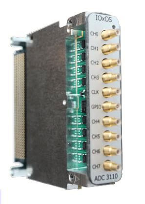
The ADC_3112 is a FMC VITA57.1 module featuring low-power high-density 12-bit/900(1000) Msps ADC capability based on TI latest generation of ADCs, the ADS5409. Thanks to on-board interleaving support and individual clock source programming, two ADC channels can be used on the same input channel, providing an astonishing 12-bit/1800 (2000) Msps sampling rate.

The four (4) analog inputs are implemented through two (2) SSMC high-frequency connectors configurable as DC coupled differential or single-ended. The high-speed (>1GHz) preamplifier stage, based on LT6409 device, supplies analog signals to the ADS5409 devices and to the analog trigger function.
The on-board clock tree is implemented with a high-precision low-jitter low-phase noise clock fully programmable controller LMK04803B. The clock reference source is selectable either from the front panel SSMC CLKREF input, from the on-board ultra-low phase noise XCO/VCXO or from the VITA57.1 “CLK0_C2M” LVDS signal.
To support the dual device interleaving, and to provide double sampling frequency (1800/2000 Msps), a programmable clock delay with sub pico-second resolution is introduced in the ADC clock paths

ADC_3112-A0 - Dual ADS5409 with on-board XCO 250 MHz

Digitizer

ADC_3112-A1 - Dual ADS5409 with on-board VCXO 100 MHz

Digitizer

FDK_3112 - FPGA VHDL Reference Design Kit

Digitizer

ADC_3112 FMC four channel 12-bit High Speed Digitizer
ADC-3112-A0 Dual ADS5409 with on-board XCO 250 MHz
ADC-3112-A1 Dual ADS5409 with on-board VCXO 100 MHz
FDK_3112 FPGA VHDL Reference Design Kit

f0eb62dd90fbdbf01277697d730c68a8^^^^^^^^^^^^^