ADC_3210 - FMC Eight Channel 14-bit Digitizer

Main features

  • Eight/Four (8/4) channels
    • 14-bit @ 1’300/625 Msps with on chip DDC
  • Single width FMC VITA 57.1-2008 / (FMC+)
    • HPC 400 (560) pins connector
    • 8.5/10.0 stacking option
    • Ten(10) SSMC front panel connectors
    • 4-7[W] typical power consumption
    • JESD204B signaling (2 lanes per ADC channel)
  • Based on latest generation ADC technology
    • AD 9695 dual 14-bit @ 1’300/625 Msps
    • Single ended AC coupling (ADC_3210)
    • Single ended DC coupling (ADC_3211)
    • JESD204B ADC read-out interface
  • Sophisticated clock tree distribution
    • TI LMK04616(dual PLL)
    • On-board ultra-low noise oscillator VCXO or Programmable XCO/VCXO
    • External SSMC Clock reference
  • On board low noise power supplies generation
  • Temperature sensor monitoring through SMBus
  • Xilinx Ultrascale/Zync+ FPGA VHDL Design Kit
  • LINUX Software Library
Price request Datasheet Ask a question

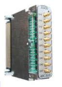
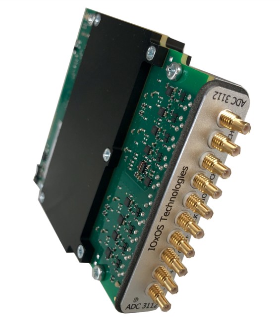
The ADC_3210/3211 is a FMC VITA 57.1-2008 / FMC+VITA 57.4-201 form factor featuring eight (8) ADC channels of 14-bit at 1’300/625 Msps.

The ADC_3210/3211 is based on latest ADC high-speed low-power generation with digital read-out through JESD204B interface, operating from 6.25 Gbps up to 13Gbps.The eight (8) single-ended 50 Ohms analog inputs are supplied through SSMC high frequency connectors. AC coupling (ADC_3210) and DC coupling (ADC_3211) versions are available.

Each ADC channel can optionally be connected to a wide-band digital down-converter (DDC) block, featuring decimation and low-pass / high-pass / band-pass filtering as well as digital I/Q mixing.

Clock tree is implemented with a high precision on-board low jitter low phase noise clock controller LMK04616, fully programmable by the carrier-board. The clock reference source is selectable from front panel SSMC input, FMC/FMC+ clock source or from an on-board ultra-low phase noise VCXO / programmable XCO. The FMC/FMC+ ADC_3210/3211 incorporates precise synchronization mechanism for the dual PLL on-board clock controller LMK04616 and/or ADC devices allowing to keep in phase several units.

A user programmable GPIO SSMB can be defined as user specific TRIGGER, GATE, on-board PLL synchronization for CLOCK replication or any user specific function embedded in the carrier FPGA. A high-speed compactor with programmable level (DAC) is inserted in the GPIO input path.

ADC_3210-XX-YY-Z-LP-A0 - FMC Eight Channel 14-bit Digitizer - AC coupling version

XX : Resolution → 14 : 14-bit YY : Speed → 06: 625 Msps / 13 : 1300 Msps Z : Channels numbers → 4 : Four channels / 8 : Eight channels LP: Low pass filter: 00: filter bypass / nn: upon customer request V : VCXO option

ADC_3211-XX-YY-Z-LP-A0 - FMC Eight Channel 14-bit Digitizer - DC coupling version

XX : Resolution → 14 : 14-bit YY : Speed → 06: 625 Msps / 13 : 1300 Msps Z : Channels numbers → 4 : Four channels / 8 : Eight channels LP: Low pass filter: 00: filter bypass / nn: upon customer request V : VCXO option

FDK_3210 - One time fee for ADC_3210/ADC_3211VHDL integration firmware (Kintex UltraScale)

ADC_3210

ADC_3210 FMC Eight Channel 14-bit Digitizer
ADC_3210-XX-YY-Z-LP-A0 FMC Eight Channel 14-bit Digitizer - AC coupling version
ADC_3211-XX-YY-Z-LP-A0 FMC Eight Channel 14-bit Digitizer - DC coupling version
FDK_3210 One time fee for ADC_3210/ADC_3211VHDL integration firmware (Kintex UltraScale)

b33a9335a72dfba38696b8cbd5db4e0ayyyyyyyyyyyyyyyyyyyyyyyyyyyyyyyy